Local and reversible restructuring on a Ge(001) surface
driven by STM below 80 K
Yasumasa Takagi, Yoshiihde Yoshimoto, Kan Nakatsuji and Fumio Komori
ref.1) Local and Reversible Change of the Reconstruction on Ge(001) Surface between c(4x2) and p(2x2) by Scanning Tunneling Microscopy, J. Phys. Soc. Japan 72 (2003) #10. ; e-preprint, http://arXiv.org/abs/cond-mat/0303522.
2) Reversible local-modification of surface structure on clean Ge(001) by scanning tunneling microscopy below 80 K, Surf. Sci. 559 (2004) 1-15.
Reversible control of local surface superstructures by STM is expected on the ground state c(4x2) reconstructed surface of Ge(001) as well as Si(001) because the energy difference between the ground state and the p(2x2) structure is estimated to a few meV/dimer.[1] We have demonstrated that the surface reconstruction on Ge(001) is locally and reversibly changed between c(4x2) and p(2x2) by controlling the sample bias voltage, Vb , of a scanning tunneling microscope (STM) below 80 K. The c(4x2) structure is observed with Vb < - 0.7 V while the p(2x2) with Vb > + 0.8 V. Moreover, the both structures can be kept under scanning the surface with |Vb| < 0.6 V after fixing the surface structure of a local area by scanning there with a higher |Vb|.
Figures 1 shows successive local modifications of the surface. After taking the image shown in Fig. 1(a), the area A in the figure was scanned with Vb = 0.8 V to change from c(4x2) to p(2x2). The result is shown in Fig. 1(b). The change along the dimer row continued to the outside of the scanning area. Then we scanned the area B in Fig. 1(b) to form another p(2x2) area as shown in Fig. 1(c). The reverse change from p(2x2) to c(4x2) was done by scanning the area C in Fig. 1(c) with Vb = - 0.7 V. In this case, we had to scan all of the desired p(2x2) area because the change to c(4x2) was limited nearby the area of the scanning along the dimer row. The annihilation of p(2x2) is shown in Fig. 1(d). The observed structure is summarized in Fig.1(e).
The observed bistability between p(2x2) and c(4x2) on Vb is attributed to the changes in two competing energies determining the structure; the electric dipole energy among the Ge dimers, and that of the subsurface lattice strain. The upper atom of the Ge dimer is negatively charged, and the dipole energy for p(2x2) structure is smaller than that for c(4x2). On the other hand, the strain energy for p(2x2) is larger than that for c(4x2). Both are affected by the electric field between the tip and the surface as schematically shown in Fig.2. For the positively biased surface, the p(2x2) structure is favoured by the gain of the dipole energy, and can be the ground state. On the other hand, under the negative Vb , the buckling of the dimers is increased by the electric field, and the c(4x2) structure is more favoured. The current dependence of the transition indicates that an inelastic scattering process during the electron tunnelling induces the transition under the electric field by STM.
References
[1] Y. Yoshimoto et al., Phys. Rev. B61, 1965 (2000).
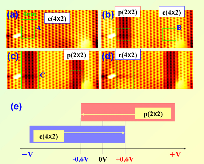
Figure 1: (a-d) Successive STM images of the same area (22.5 x 10 nm2) of a Ge(001) surface at 80 K with Vb = - 0. 2V. The square areas "A" in (a) and "B" in (b) were scanned with Vb = 0.8 V to change the local structure from c(4x2) to p(2x2) after taking each image. The surface after scanning "A" is shown in (b), and that after scanning "B" is in (c). The rectangular area "C" in (c) was scanned with Vb = - 0.7 V to change it from p(2x2) to c(4x2). The surface after scanning the area "C" is shown in (d). (e) A schematic showing the observed structures depending on the bias voltage and the direction.
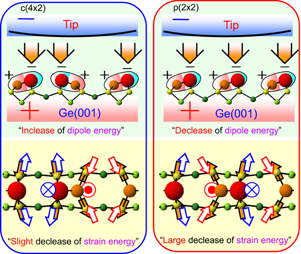
Figure 2: When the surface is positively biased under the STM tip, the negatively charged upper-atoms of the dimers are electro-statically pushed toward the subsurface by the tip, and the lower-atoms are pulled toward the tip. Consequently, the dimer buckling becomes smaller. This makes the difference of the subsurface strain energy between c(4x2) and p(2x2) structures smaller than that of the dipole energy among buckled dimers. Thus for the positively biased surface, the p(2x2) structure is favored by the gain of the dipole energy, and can be the ground state.