An Atomic Seesaw Switch for One-Dimensional Electrons on Ge (001)
K. Tomatsu, Y. Takagi, K. Nakatsuji, H. Kusuhara, A. Ishii and F. Komori
Reversible switching of electronic conduction through atom manipulation is one of the main subjects of nanoscience. However, different conducting pathways have not been clearly observed with atomic resolution. We demonstrate the correlation between the change of surface atomic position and that of the reflection of one-dimensional (1D) surface-state electrons on the Ge (001) surface with a low coverage of Sn atoms [1].
On the clean Ge(001) surface, two atoms form a buckled dimer, and bonding pi- and antibonding pi*-states localize on upper and lower atoms of the dimer. The Ge dimers align in the [110] direction and form a dimer row. The pi*-electron behaves like a 1D free electron along the dimer row (see Fig. 1). The buckling orientation of the Ge dimer can be reversibly controlled by surface bias voltage of STM below 80 K [2].
When Sn atoms are deposited on the clean Ge(001) surface at room temperature, buckled dimers originating from the Sn atoms are formed at the Ge dimer position in the surface [3]. The contrast of the STM dimer image at 80 K changes by reversing its buckling orientation as shown in Fig. 2. Thus, it is identified as a heterogeneous Sn-Ge dimer. On the basis of first-principles calculations, the optimized structure of the heterogeneous dimers is estimated. The most stable structure is the buckled dimer with the Sn atom at the upper dimer position (U dimer). The energy of the dimer with the Sn atom at the lower dimer position (L dimer) is 60 meV higher than the ground state.
An atomic seesaw switch is realized for the 1D pi* electrons in the Ge dimer-row direction by using STM to flip reversibly the buckling orientation of a single Sn-Ge dimer in the dimer row at 80 K. When the Sn atom of the heterogeneous dimer is at the lower position (L dimer), the 1D electrons are reflected and a standing wave of this state is observed in the dI/dV image as in Fig. 1(b). Whereas, when it is at the upper position (U dimer), the 1D electrons pass through the heterogeneous dimer, and no standing wave is observed as in Fig. 1(e). In this state, the lower atom of the dimer is Ge, and the pi* state of the dimer is little different from that of the Ge-Ge dimers.
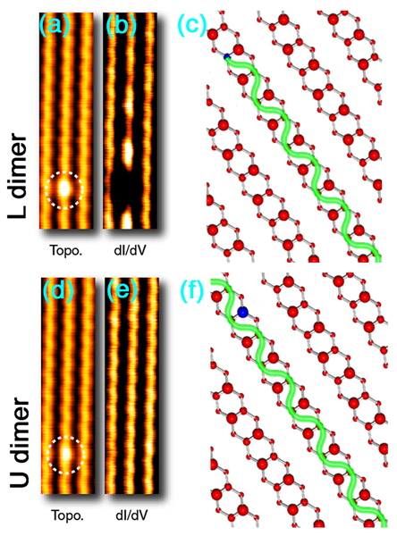
Fig.1 (a,b) Topographic (a) and dI/dV (b) images of the Ge(001) surface with L dimer at 80 K. The L dimer is imaged as a protrusion in the topographic image, and a standing wave is observed around the L dimer in the dI/dV image. (c) Schematic illustration showing the pi*-electrons (green line) , which conduct on the lower atoms of the Ge dimers in the dimer row directon [110], are reflected by the Sn atom (small blue ball) at the lower dimer position. Red balls indicate the Ge atoms. Large balls are the upper dimer atoms, and small ones the lower. (d,e) Topographic (d) and dI/dV (e) images of the Ge(001) surface with the U dimer at 80 K. The U dimer is imaged as a protrusion in the topographic image while no standing wave is observed around the U dimer in the dI/dV image. (f) Schematic illustration showing the pi*-electrons (green line) can go through the Sn-Ge dimer. The Sn atom (large blue ball) at the upper dimer position little affects the pi*-electron conduction.
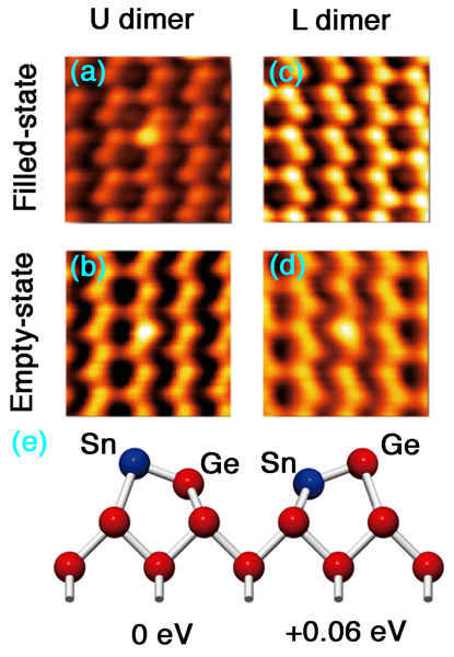
Fig.2 (a-d) Filled (Vb = - 0.5 V) and empty (Vb = + 0.5 V) state STM images for the Sn-Ge dimers with the Sn atom at the upper (U dimer) and lower (L dimer) positions on the Ge(001) surface. Brightly imaged protrusions indicating the Sn-Ge dimer are seen in (a,b,d) while its image is the same as the Ge-Ge dimer in (c). Local superstructure of the surface changed as reversing the buckling orientation of the Sn-Ge dimer. (e) Structural models of the U dimer and the L dimer. The energy of the L dimer is 0.06 eV higher than that of the U dimer.
References
1. K. Tomatsu et al, Science 315 1696 (2007).
2. Y. Takagi et al, J. Phys. Soc. Jpn. 72 2425 (2003).
3. K. Tomatsu, et al., Surf. Sci. 601 1736 (2007).