Hole Injection Induces Local Motion of Surface Atoms through Electron-lattice Interaction
K. Tomatsu, K. Nakatsuji, M. Yamada, B. Yan, C. Yam, Y. Xu, T. Frauenheim, W. Duan, and F. Komori
Strong excitation of local vibration can induce the motions of atoms and molecules in various materials. The most effective way to realize the highly excited vibration is to convert electronic excitation to vibrational one through the coupling between them. Moreover, the electronic excitation at extended states can realize a nonlocal manipulation of the atoms and molecules. At the clean Ge(001) surface, the carriers injected into the surface states reversibly and nonlocally alter the tilting orientation of the Ge dimers. [1] The change rate linearly depends on the tunneling current for both the electron and hole injections, indicating the single electron excitation process. Using scanning tunneling microscopy (STM) and density functional theory, we have studied the microscopic processes of this nonlocal atom manipulation through the surface electronic excitation induced by hole injections. [2].
Figure 1 shows STM images and models illustrating the change of the dimer tilting orientation. We can continuously monitor the local structure change as the tunneling current increase or decrease when the STM tip is fixed. Actually, the creation of the kink pair shown in Fig. 1(b) was detected at the positions above the points A-D as different values of the tunneling current. With increasing the excitation energy of the injected hole, the kink creation rate per electron first increases, once saturates, and then increases again as shown in Fig. 2(a). The electronic states (Fig. 2(b)) and their coupling to two rocking modes of the adjacent dimer pair, out-of phase and in phase as illustrated in Fig. 2(c), were calculated for understanding the observed rate of the kink creation. The both modes strongly couple the unoccupied π*, occupied π and σ states of the dimers, and the occupied dimer back-bond states. The dimer orientation change is mainly induced by the carriers injected to the π* and π states. The observed two-step increase of the creation rate by the hole injection is attributed to the crossover of the electronic states from the π to σ. The hole injected to the B1 state induces the rocking mode vibration, but its energy is not enough to induce the change of the tilting orientation.
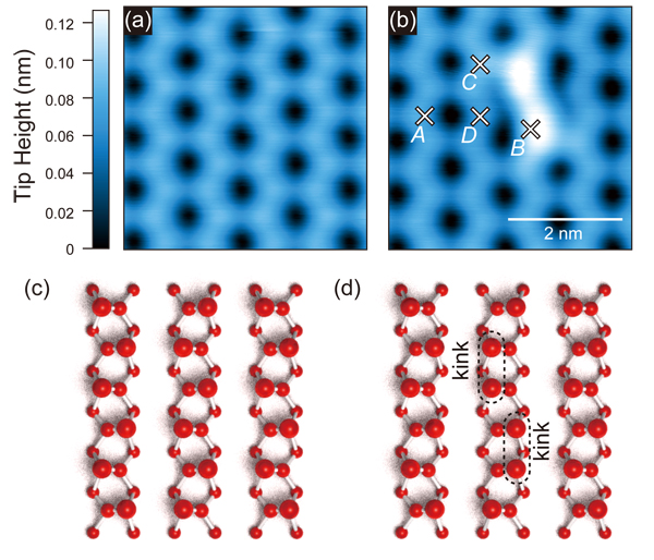
Fig. 1 Topographic STM images of the clean Ge(001) surface at 80 K before (a) and after (b) creation of a kink pair by hole injection at the sample-bias voltage, Vb = - 0.7 V. The corresponding ball models for the clean surface and the kink pair are given in (c) and (d). Large, middle, and small balls represent upper dimer, lower dimer and second layer Ge atoms. At Vb = - 0.5 V, the kinks were stable, and imaged higher than the Ge dimers as in (b). The kink pairs are not always created in the dimer row including the tunneling point as schematically shown as the cross B, but in the neighboring dimer rows. The creation of the pair at the dimer row with the cross B can be detected as the change of the tunneling current at the crosses A, C and D.
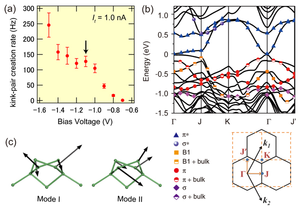
Fig. 2 (a) Kink pair creation rate as a function of the bias voltage during the hole injection. (b) Calculated band structure of the clean Ge(001) with the c(4x2) reconstruction. Band characters, the π*, π and σ states of the dimers, the dimer back-bond state (B1), and their mixing of the bulk states, are shown. Atomic structure of a slab model with 10 Ge layers was optimized. (c) Displacement vectors of the dimer atoms in the neighboring Ge dimers for two rocking modes, out of phase (left) and in phase (right). These two modes couple the surface electronic states.
References
1. K. Takagi et. al.; Surf. Sci. 559, 1 (2004).
2. K. Tomatsu et. al.; Phys. Rev. Lett. 103, 266102 (2009).