Remote atomic manipulation of dimer buckling through carrier propagation in the surface states
Y. Takagi, Y. Yoshimoto, K. Nakatsuji and F. Komori
Electronic excitation induced by tunneling electrons in scanning tunneling microscopy (STM) often moves the atoms under the tip. On the clean Ge(001) surface, it locally inverts the buckling orientation of the Ge dimers without cutting the Ge bond below 80 K [1]. Moreover, we can reversibly control the orientation to change the area of local c(4x2) or p(2x2) structures by selecting the sample bias voltage Vb in the STM operation. The two different local structures coexist on the same surface when Vb is between - 0.6 V and 0.7 V. In the other range of Vb, one of the two structures covers the whole surface when it is scanned by the STM tip. The mechanism of the transformation is explained by a coherent climbing of the vibrational state of the dimer by electronic excitation [2].
The electron tunneling from or to the STM tip remotely creates and moves a metastable topological defect between c(4x2) and p(2x2) shown in Fig. 1. Hot electrons or holes created in the Ge surface states by the tunneling propagate along the surface, and induce the defect motion in the dimer row direction through the electron-lattice interaction, as demonstrated in Fig. 2. The direction of its motion depends on the electric field due to STM bias through the electric dipole of the Ge dimer. We have measured the rate of the defect motion induced by tunneling electrons as functions of the distance and the direction between the defect and the tunneling point, and the bias voltage during the pulse. The threshold distance of the motion rapidly increases with increasing the absolute value of the bias voltage for the both polarities. It is much longer in the dimer row direction than in the dimer direction for the transformation by electron injection. On the other hand, the distance is almost isotropic for the transformation by hole injection. The difference is attributed to that in the lifetime of the excited carriers in the surface electronic states on the basis of the band calculation. [3]
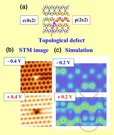
Fig.1 (a) Schematic model of the topological defect between c(4x2) and p(2x2) areas on the Ge(001) clean surface. (b) STM images of the defect for two sample bias voltages. The image area is 6 nm x 6 nm. (c) Simulated STM images including the defect (red circle) on the basis of the first-principles calculation
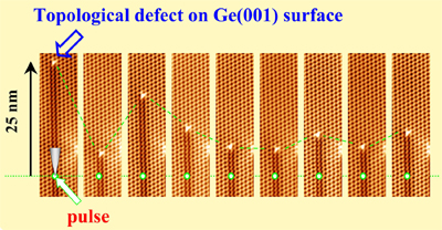
Fig.2 STM images showing one-dimensional motion of the topological defect on the Ge(001) surface by pulse current injection. Each time after the injection of electrons from the STM tip at the point of the green circle, the defect moves in the dimer-row direction. The center of its random walk is 8 nm apart from the point of the electron injection by the bias voltage pulse to 0.8 V. The center position separates further with increasing the bias voltage during the electron injection. When we decrease the bias voltage below 0.7 V, the defect comes just under the STM tip.
References
1. Y. Takagi, Y. Yoshimoto, K. Nakatsuji and F. Komori, J. Phys. Soc. Jpn. 72, 2425 (2003), 74, 3143 (2005), Surf. Sci. 593, 113 (2005).
2. H. Kawai and O. Narikiyo, J. Phys. Soc. Jpn. 73, 2362 (2004).
3. K. Nakatsuji, Y. Takagi, F. Komori, H. Kusuhara and A. Ishii: Phys. Rev. B72, 241308(R) (2005).