Graphene π-bands on Si-terminated Vicinal SiC(0001)
K. Nakatsuji, Y. Shibata, R. Niikura, K. Morita, S. Tanaka, F. Komori
Massless π bands of graphene grown on a SiC(0001) substrate can be modified by the scattering at the boundaries and the interface superstructure. We investigated the π band structure and width of the single- and double-layer grown on a Si-terminated vicinal SiC(0001) substrate using angle-resolved photoemission spectroscopy (ARPES). The π electron scattering at the substrate steps makes the spectrum width anisotropic, but no difference in the π band shape. Quasi-2×2 replicas of the π band due to the interface 6√3×6√3-R30° superstructure were observed in the single-layer graphene while they were absent in the double-layer graphene.
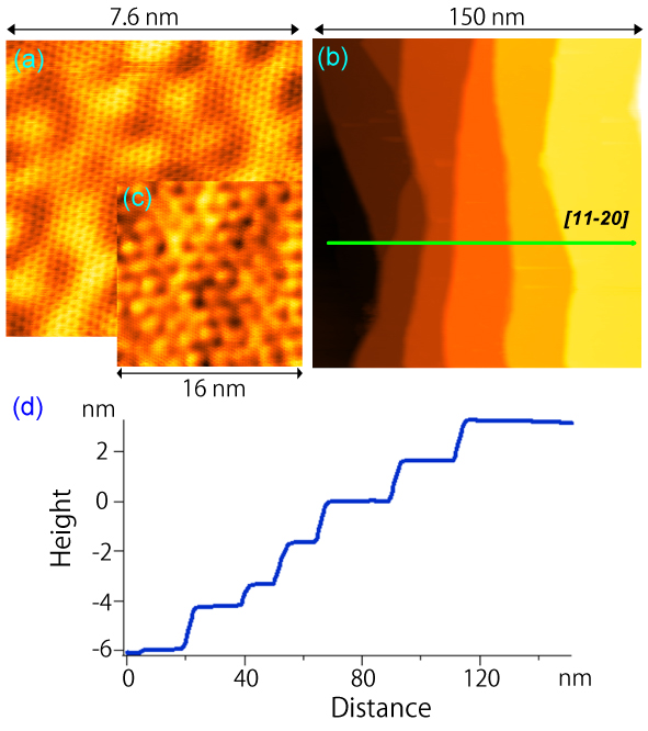
Single- and double-layer graphenes were grown on Si-terminated surface of nitrogen-doped 6H-SiC(0001) substrates vicinal to the [11-20] (4° off) direction. [1] The substrate surface was first etched in H2 gas, and a SiON thin film [2] was successively formed on the surface by annealing in N2 gas. Finally, graphene layer was made on this substrate by annealing in N2 gas over 1900 K for up to a few hundred sec. The average thickness of the graphene can be controlled by the annealing temperature and time. The STM images of the graphene are shown in Fig. 1. The graphene covers all the substrate including the step-edge areas.
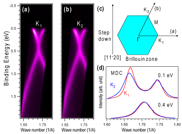
Figure 2 shows the results of ARPES.[3] The π band spectrum in the direction perpendicular to the step-down direction (K1) has a narrower width in the momentum distribution than the band in the other direction (K2) when the binding energy from Fermi energy EF is smaller than 0.2 eV. However, there is no significant difference in the π band shape between them. The anisotropy of the line width is attributed to the π electron scattering at the curved areas on the substrate step edges. The origin of the observed nonlinear dispersion of the π band is not due to the electron scatterings at defects of the graphene, but to the many-body effects and/or the electronic potential due to the interface 6√3×6√3-R30° structure of carbon atoms, which cause the quasi-2×2 replica π bands in ARPES.

Fig. 1(a-c) Topographic STM images of single-layer graphene grown on the Si-terminated SiC(0001) substrate vicinal to [11-20] direction. The hexagonal atomic arrangement and the interface 6√3×6√3-R30° superstructure can be seen for magnified images (a,c). A step-and-terrace structure is evident in the image of a wide area (b). The images were taken at 80 K. (d) Cross section along the line in (c).

Fig.2 (a,b) π band structures at two K points measured by ARPES for single-layer graphene grown on the SiC(0001) substrate vicinal to [11-20] direction. (c) Graphene Brillouin zone, and definitions of the K1 and K2 points. The Γ-K1 direction is perpendicular to the step-down direction, and the Γ-K2 direction is 30° rotated from the step-down direction. (d) Momentum distribution curves at 0.1 and 0.4 eV below EF for the π band spectra around K1 and K2. At 0.1 eV, the line width around K1 is narrower than that around K2 while it is almost the same at 0.4 eV.
References
1. S. Tanaka, et. al., Phys. Rev. B 81, 041406(R) (2010).
2. T. Shirasawa, et. al., Phys. Rev. Lett. 98, 136105 (2007).