Atomic Switch for Scattering Phase of Electrons at Ge (001) Surface
K. Tomatsu, B. Yan, M. Yamada, K. Nakatsuji, W. Duan, F. Komori
An electron changes its phase when it is scattered by an atomic potential. The scattering phase shift can be detected on the metal and semiconductor surfaces by observing the electron standing wave in the differential conductance (dI/dV) image using scanning tunneling microscopy (STM). We have studied the reflection phase of one-dimensional (1D) electrons at four kinds of atomic potentials on the clean Ge(001) surface. The clean Ge surface consists of buckled dimers, which align in the [110] direction and form dimer rows. The empty π*-band electrons of the surface Ge dimers behave like 1D free electrons along the dimer row. We measured the π*-band standing waves around the buckled dimer with one Si or Sn atoms in the differential conductance images at various sample-bias voltages.
Figure 1 shows the topographic STM images of the Si-Ge dimers on the surface at 80 K. Two kinds of buckled dimers with a Si atom at either the upper or lower position (Si U- and L-dimers) are made by deposition of Si atoms on the clean surface at room temperature as in the models. These dimers can be distinguished by observing their sample-bias dependence. Standing waves appear and decay from the both kinds of the impurity dimer. The cross sections of the dI/dV images from the Si-Ge dimers are shown in Figs. 2(a). The standing waves due to a Sn-Ge L-dimer with a Sn atom at the lower position (Sn L-dimer) [1] are shown in Fig. 2(b) for comparison. The scattering phase of Si L-dimer has the sign opposite to those of Sn L-dimer and Si U-dimer. The results indicate the scattering potential by Si L-dimer is attractive while the potentials due to other two impurity dimers are repulsive. The signs of the scattering potential are reproduced by first-principles calculations. The difference between Si and Sn L-dimers is attributed simply to energy difference of the valence pz states among Si, Ge and Sn atoms. [2] We are able to transform one kind of the Si-Ge dimer to the other kind reversibly by changing the bias polarity together with the buckling orientation of all the Ge dimers in the dimer row including the impurity dimer. Thus, using the Si-Ge dimer, we have realized a scattering phase switch in an atomic scale.
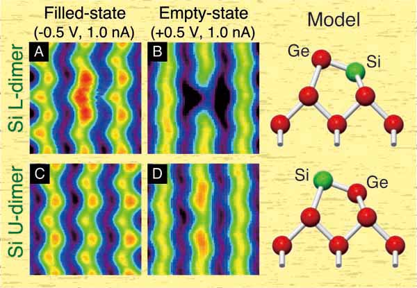
Fig. 1 Topographic (A-D) STM images of Si U- and L-dimers on the Ge(001) surface at 80 K for two sample-bias voltages ± 0.5 V. At + 0.5 V, the both dimers are lower than the pure Ge dimer while at - 0.5 V, Si L(U)-diner is higher than (has the same apparent height as) the pure Ge dimer. We identified the both dimers by comparing these STM images with the local electronic states obtained by DFT calculations for their optimized atomic structures. The corresponding schematic models for the dimers are given in the left column.
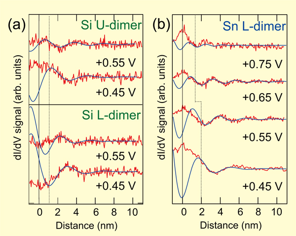
Fig. 2 Red curves are cross sections of the standing waves of the 1D π* electrons in the dI/dV images for Si L- and U-dimers (a) and Sn L-dimer (b) at several sample bias voltages. The data were obtained at 80 K. The dimer is at the origin of the abscissa in each figure. Each blue curve is the damping oscillation fitted to each red curve. For the fitting, we used the dispersion relation of the π*-band obtained on the clean surface.
References
1. K. Tomatsu, K. Nakatsuji, T. Iimori, Y. Takagi, H. Kusuhara, A. Ishii, and F. Komori, Science 315, 1696 (2007).
2. K. Tomatsu, B. Yan, C. Wang, M.Yamada, K. Nakatsuji, G. Zhou, W. Duan, and F. Komori, Phys. Rev. B 78, 081401(R) (2008).