|
I am studying dynamics, self-assembly, and electric states of nano-structures
on semiconductor surfaces with scanning tunneling microscopy (STM) at Institute
for Solid State Physics (ISSP), the University of Tokyo. In the following,
I will briefly introduce my research subject. The copyright of the images
on the present page is retained by Kota Tomatsu and Komori laboratory at
ISSP, and redistribution and copy are not allowed.
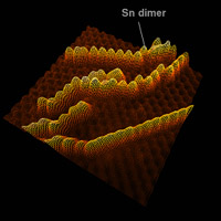
Growth of Sn dimer chains on a Ge(001) surface
We have revealed that when submonolyer of Sn atoms is deposited onto Ge(001), self-assembled 1D structures composed of Sn ad-dimers, so-called "dimer chains", are formed. The following image is of a STM image exhibiting the Sn dimer chain on Ge(001) surface. The direction in which the Sn dimer chain extends depends is governed by a surface diffusion barrier of Sn adatoms, and the barrier correlates with a surface strain.
References:
"STM observation of initial growth of Sn atoms on Ge(001) surface"
K. Tomatsu et al., Surf. Sci. 601, 1736-1746 (2007)
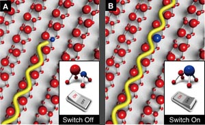
An atomic seesaw switch formed by a Sn-Ge dimer on a Ge(001) surface
The clean Ge(001) surface is composed of tilted dimers. We found by flipping
the tilting orientation of surface dimers with STM that the deposited Sn
atom incorporates into the substrate and forms a heterogeneous Sn-Ge dimer
at the Ge dimer position. On the Ge(001) surface, one-dimensional free-electronic
states are realized. We have demonstrated that the current flow on the
surface can be controlled by the bistable Sn-Ge dimers, which oppositely
tilt to each other. This result can be regarded as realization of an "atomic
seesaw switch" as shown in the following figure. The red and blue
atoms represent Ge and Sn atoms, and a yellow curve represent an electron
pathway. A movie file demonstrating the atomic seesaw switch realized by
the Sn-Ge dimer is available here.
References:
"An Atomic Seesaw Switch Formed by Tilted Asymmetric Sn-Ge Dimers on a Ge(001) surface"
K. Tomatsu et al., Science, 315, 1696-1698 (2007).
Notes:
The image is posted by permission of the AAAS for personal use.
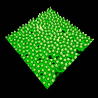
Development of analysis software for scanning probe microscopy
I am developing an analysis software for scanning probe microscopy, "EasySPM",
for myself and my colleagues. This work is unofficial and private. I will
design frontier analysis methods through this work. The image presents
a three-dimensional view of a Si(111) surface rendered with EasySPM.
Notes:
EasySPM is available for download on the present website. For details,
see here.
|
|