Home
Research-1:
Topological insulators and nanostructured graphene
Research-2: Semiconductor Surfaces
Research-3:
Nano Ferromagnet and Metal Surfaces
Member
Selected publications
Main equipment
ISSP home
Nano Ferromagnet and Metal Surfaces
Research 3: Nano Ferromagnet and Metal Surfaces
Systematic image change of STM with the tip-surface distance is observed on the ferromagnetic monatomic layer Fe2N grown on the Cu(001) surface. The origin is attributed to the distance-dependent shift of the electronic states predominant in the tunneling process between the Fe-3d and sp states. (details)
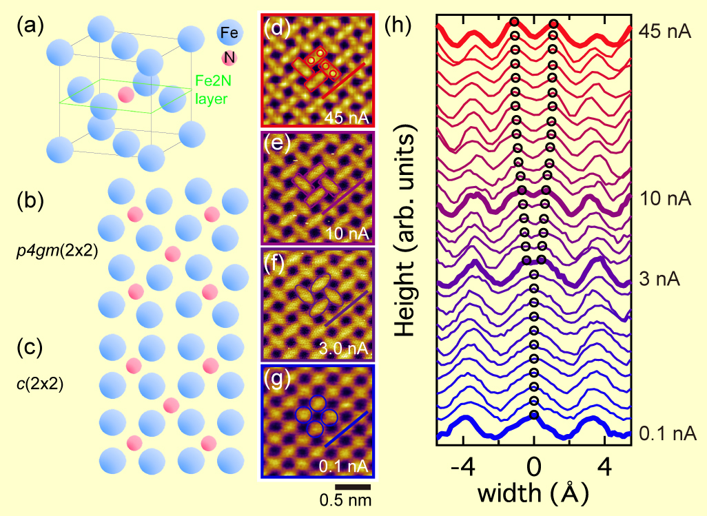
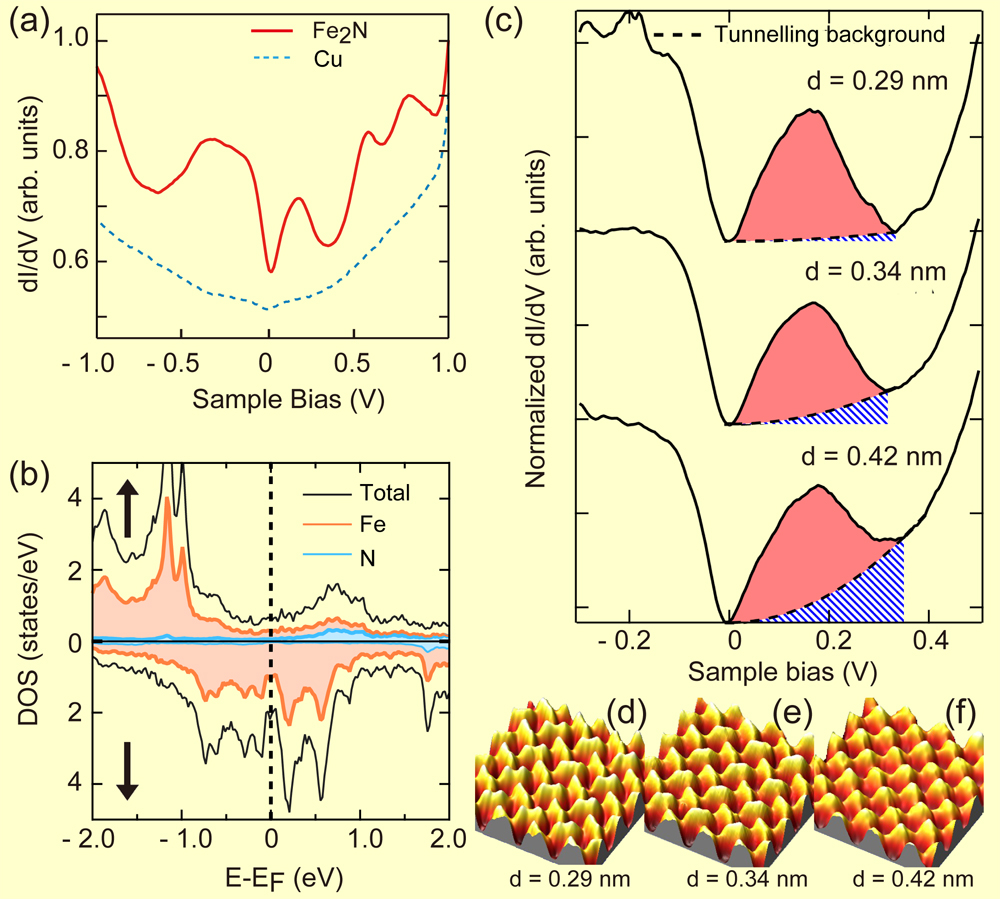
Left (a-c) Schematic models of the bulk Fe4N crystal (a) and of Fe2N monolayer (b,c). (d-h) Topographic images and line profiles taken at various values of the tunneling current. Right(a) dI/dV spectrum of monolayer Fe2N on Cu (001) and the clean Cu(001) surface. (b) Calculated spin-resolved LDOS of monolayer Fe2N on Cu(001). (c) Distant-dependent dI/dV spectra, and (d-f) corresponding STM images.
Epitaxial fcc Fe overlayer is stablized against transformation towards the bulk stable bcc phase with increasing the Fe coverage on the Cu(001) surface. The stablization is attributed to the relief of the lattice strain by the step edges. (details)
STM images of the surface of an Fe film grown on a vicinal Cu(001) surface. Dotted lines indicate substrate step edges. (a) Image including three steps. (b) High-resolution image indicating growth of an fcc Fe film with a square surface lattice on a narrow terrace. Large protrusions on the terrace are adsorbed CO atoms. (c) High-resolution image indicating growth of both the fcc Fe film and an Fe film with complicated surface structure on a wide terrace. On the surface of lower terrace, the right region has a square lattice, and the left complicated lattices. About 80 % of the latter surface is covered by CO atoms forming local 2 x 2 structures. (d) Magnified image of the fcc Fe surface. (e-g) Magnified images of the left region in (c) with adsorbed CO atoms. Square (e), p2mg(2 Å~ 1) (f) and, nano-martensitic (g) lattices are recognized.
Tin-adsorbed Cu(001) surfaces exhibit various atomic super structures depending on the Sn coverage. Six ordered phases with metallic surface states have been confirmed by STM and LEED. The surfaces with 0.375 and 0.5 ML coverage of Sn show metal-insulator transitions.
STM images of Sn-adsorbed Cu(001) surfaces.
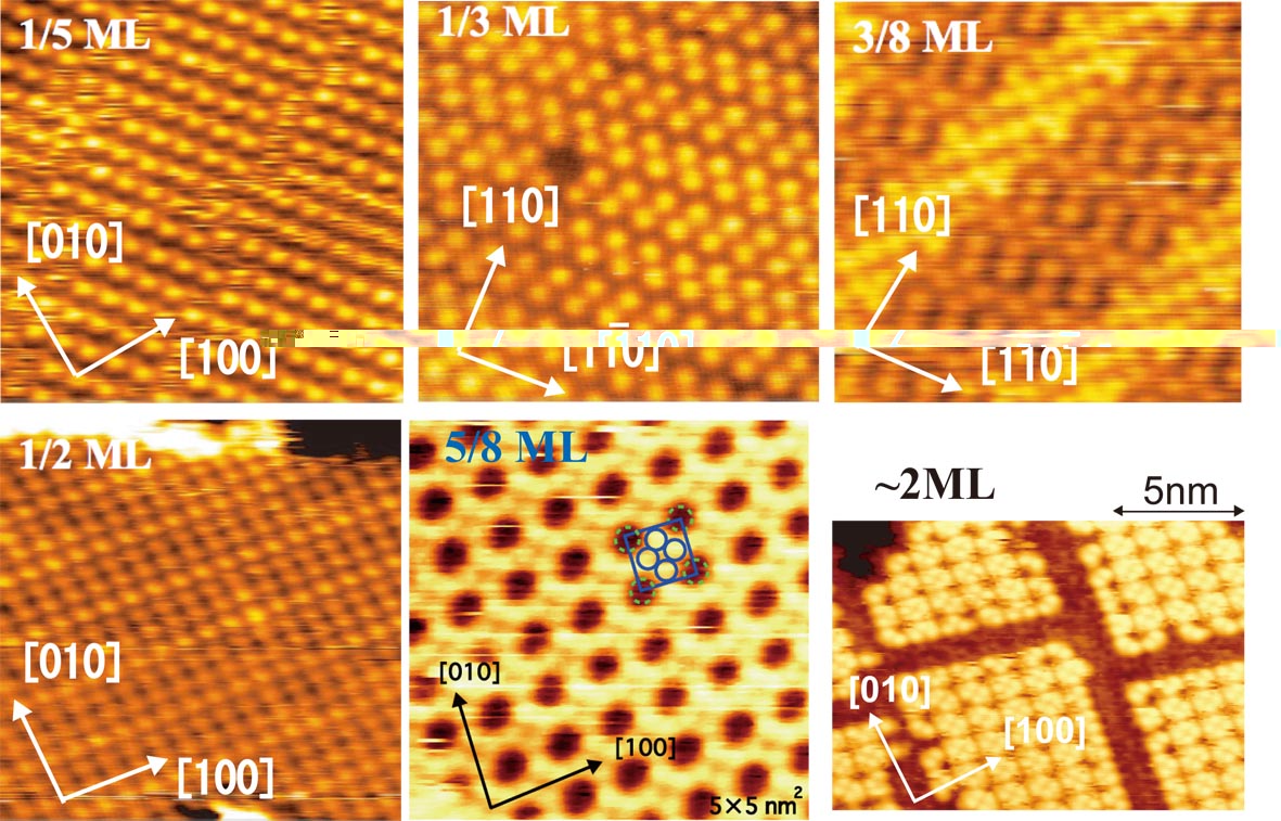
Self-assembled manganese nitride nano-islands are formed on the Cu(001) surface. (details) The presence of the MnN strips surrounding the MnN island can minimize the total lattice-strain energy. The MnN island is stabilized by such a simultaneous bilayer organization.
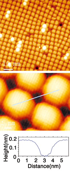
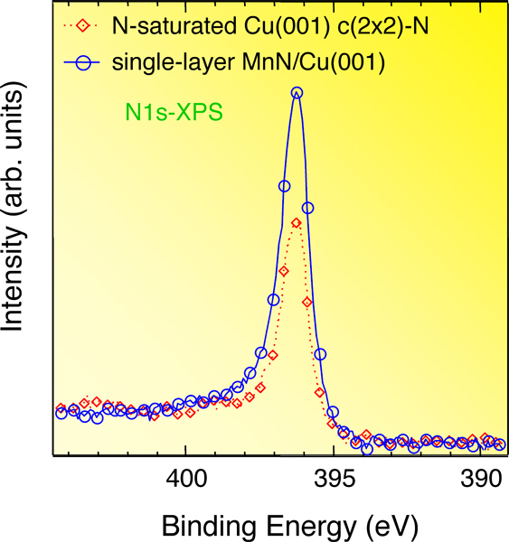
Self-assembled MnN nanoislands (left) and N-1s core-level spectra from a N-saturated Cu(001)c(2x2)-N surface and a single-layer manganese nitride covered surface (right)
Direct evidence of the strain-induced change of individual Cu3d states is observed by angle-resolved photoemission spectroscopy. (details) Energy level and the holding point of the 3d Tamm state at M shift with increasing the lattice-strain. Whereas, the energy of the d-band bottom decreases.
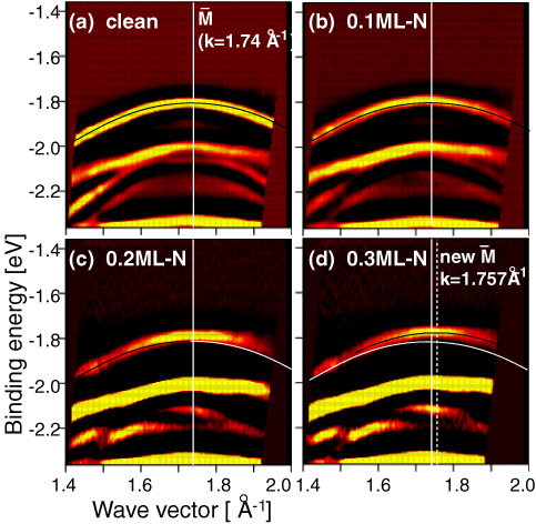
STM image of a grid pattern on a nitrogen adsorbed Cu(001) surface (left) and band structures around M for 4 kinds of nitrogen adsorbed Cu(001) surfaces (right)
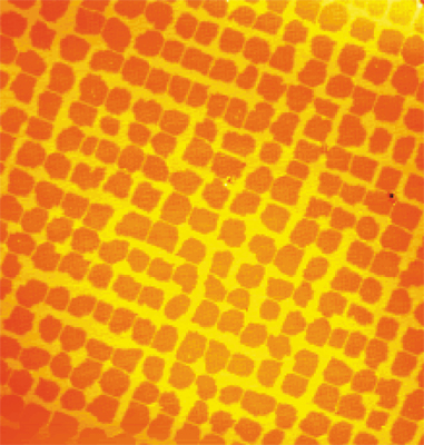
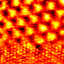
Novel periodic nanopatterns on vicinal N/Cu(001) surfaces are explored by STM . (details) The driving force for their formation is attributed to competing two strain-relief mechanisms, lines with clean Cu surface and step-edges.
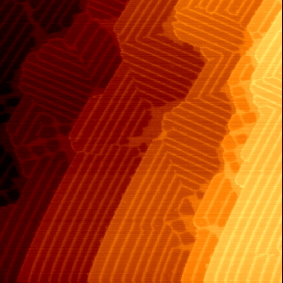
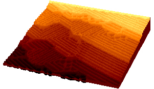
STM image of a stripe pattern on a nitrogen adsorbed vicinal Cu(001) surface.
Ferromagnetism of Co nano-particles arranged squarely on a N-adsorbed Cu(001) surface is studied using magneto-optical Kerr effect. With increasing the interaction between the particle, transition from superparamagnetism to ferromagnetism takes place. Island growth of Co and Fe on the N-adsorbed Cu(001) surfaces has been studied by STM and LEED at room temperature.
STM image of a two-dimensional array of Co nano-dots on a nitrogen adsorbed Cu(001) surface.
On a cleaved surface of a NbSe2 crystal, small areas are found with a new superstructure and a gap in the density of state around Fermi at 4.2 K. These are ascribed to a charge density wave of small NbSe2 crystals whose structure is different from the well-known bulk crystal. Tunneling spectra are taken around small iron islands on the superconducting NbS2. Superconductivity is locally destroyed by the magnetic interaction.
STM image of the surface of NbSe2 with a new CDW at 4.2 K.