Home
Research-1:
Topological insulators and nanostructured graphene
Research-2: Semiconductor Surfaces
Research-3:
Nano Ferromagnet and Metal Surfaces
Member
Selected publications
Main equipment
ISSP home
Nano Ferromagnet and Metal Surfaces
Research 2: Semiconductor Surfaces
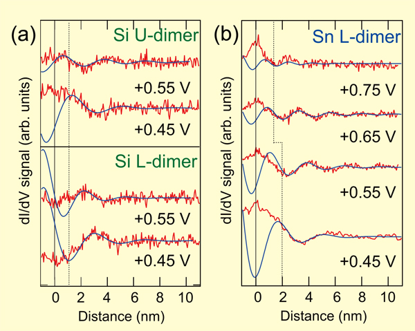
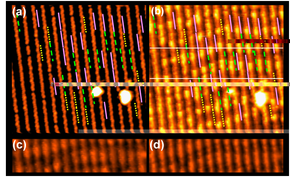
When Sn (Si) atoms are deposited on the clean Ge(001) surface at room temperature, buckled heterogeneous Sn-Ge (Si-Ge) dimers are formed at the Ge dimer position in the surface. The most stable structure is the buckled dimer with the Sn atom at the upper dimer position (U dimer). The energy of the dimer with the Sn atom at the lower dimer position (L dimer) is 60 meV higher than the ground state. An atomic seesaw switch is realized for the 1D electrons (details) in the Ge dimer-row direction by using STM to flip reversibly the buckling orientation of a single Sn-Ge dimer in the dimer row at 80 K. The 1D electrons are reflected by L dimer, and a standing wave of this state is observed in the dI/dV image. Whereas the 1D electrons pass through the U dimer, and no standing wave is observed. In this dimer, the lower atom of the dimer is Ge, and the π* state of the dimer is little different from that of the Ge-Ge dimers. In the case of Si-Ge dimers on Ge(001), the scattering amplitude is almost the same for both the Si-Ge U and L dimers while the scattering phase or potential sign is opposite (details) . Consequently, an atomic switch for the scattering phase is realized.
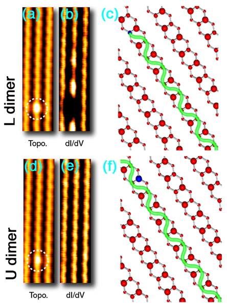
Topographic and dI/dV images of the Ge(001) surface with Sn-Ge dimers at 80 K, schematics of 1D electron conduction and the cross-sections of the standing waves.
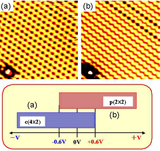
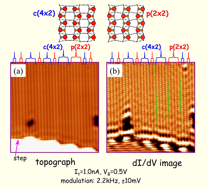
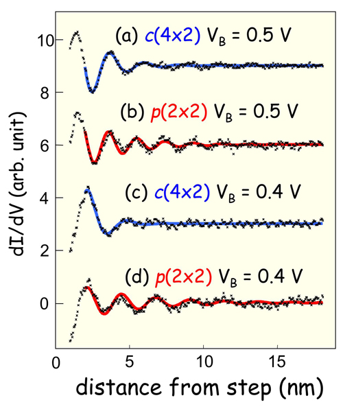
The surface reconstruction on Ge(001) is locally and reversibly changed between c(4x2) and p(2x2) by controlling the sample bias voltage, Vb , of a scanning tunneling microscope (STM) below 80 K. (details) The c(4x2) structure is observed with Vb < - 0.7 V while the p(2x2) with Vb > 0.8 V. Moreover, the both structures can be kept under scanning the surface with |Vb| < 0.6 V after fixing the surface structure of a local area by scanning there with a higher |Vb|. The transition rate depends on both Vb and the tunneling current. The observed bistability between p(2x2) and c(4x2) on Vb is attributed to the changes in two competing energies determining the structure; the electric dipole energy among the Ge dimers, and that of the subsurface lattice distortion. Both are affected by the electric field between the tip and the surface. The current dependence of the transition indicates that its origin is an inelastic scattering process during the electron tunneling under the electric field by STM. The surface electronic states strongly couple with two dimer rocking vibration modes, and the electronic energy is transferred to the local lattice system efficiently through this coupling. (details) Using pulsed change of Vb, we can make artificial surface superstructures and write nano-characters repeatedly on the same surface.
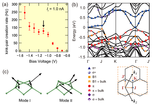
Hysteresys loop of the superstructure (left), kink creation rate vs. bias voltage (right, a), surface band structure (right, b), and two dimer rocking modes (right, c)

ISSP on Ge(001) & artificial 12x2
The microscopic process of the superstructure manipulation below 80 K was clarified as systematic creation and motion of topological defects on the surface. (details) The defect is formed and moved by hot carriers injected into the surface states from the STM tip.
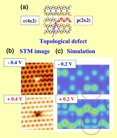
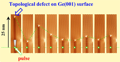
A topological defect & its motions
The dangling bond surface states on this surface were studied by ARUPS and standing wave observations. (details) The inelastic scattering of the empty state was observed as a decay of the standing wave. (details)
Surface electronic structure on Ge(001)
Dumping of standing waves on Ge(001)
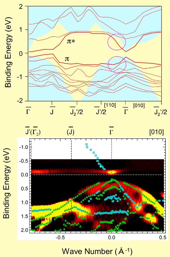
Platinum-adsorbed Ge(001) surface consists of a one-dimensional (1D) chain structure and has an ideal 1D metallic surface band. The electronic states were studied by ARPES at 6 K, a sufficiently lower temperature than its structural phase transition at 80 K, using single-domain samples. There is no gap opening at EF, indicating the 1D band does not directly contribute to the structural phase transition at 80 K. The observed spectral shape agrees with the normal Fermi-Dirac-type distribution function without any indication of a Luttinger liquid (details) .
STM images and 2D surface band of Pt/Ge(001) (details)
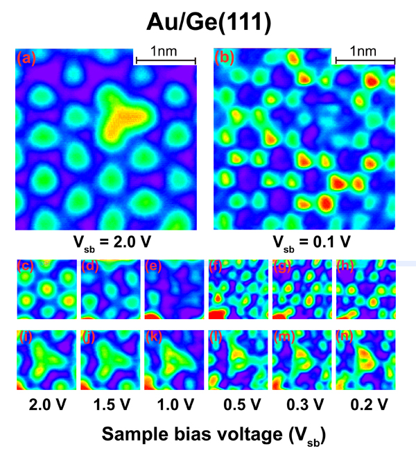
Gold-adsorbed Ge(001) surface consists of a one-dimensional chain structure in the <110> direction, and has a metallic surface electronic state. In spite of the apparent atomic structure, the surface state is two dimensional, and the dispersion perpendicular to the atomic chain is steeper than that parallel to the chain. This was demonstrated by ARPES in a single-domain surface (details) , and bias-dependent STM images (details) .
STM images, LEED patterns and 2D surface band of Au/Ge(001) (details)
Atomic and bias-dependent STM images of Au/Ge(001) (details)
Atomic and electronic structures of the gold-adsorbed Ge(111) surface are studied by STM and ARPES. The observed STM images and electronic states including the surface bands are consistent with the structure model of an optimized conjugate honeycomb-chained-trimer. Quantitative differences between the experimental and theoretical results are attributed to the doping by triangular nanoclusters observed on the surface (details) .
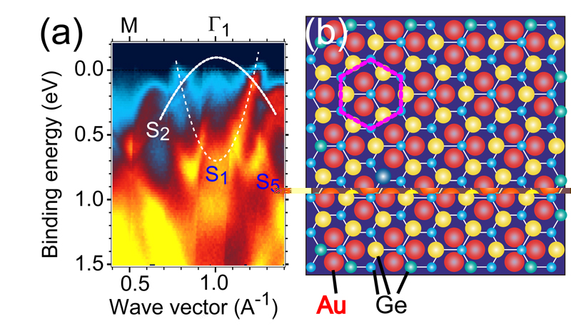
(left) Band mapping (a) and atomic structure model (a) of Au/Ge(111). (right) Atomic and bias-dependent STM images. (details)
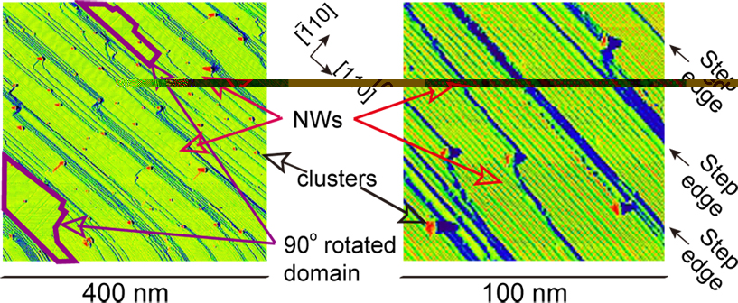
Using a home-made ultra-high vacuum low-temperature scanning tunneling microscope (UHV-LT-STM), a few mono-atomic layers of Ag on Ge(001) is studied as one of the possible superconductors specific to surface because these two materials do not form bulk alloy. Tunneling spectra on flat islands of this surface is consistent with superconductivity below 4 K. Novel thin and small structures of Ag on Ge(001) surface are observed by a room-temperature STM, and their formation process is studied using a low temperature STM.
STM image of a Ge(001) surface covered with 1ML thick Ag islands.
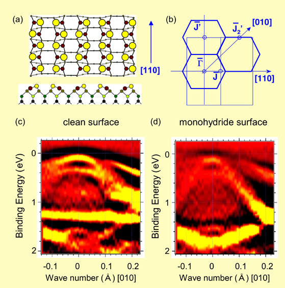
At room temperature, UV laser-induced changes of chlorine or hydrogen adsorbed Si(111) surfaces are studied by photo-electron spectroscopy and STM. By irradiation, silicon chlorides desorbe from Cl-adsorbed surfaces, while hydrogen atoms or molecules desorb from H-adsorbed surfaces. Chlorine-hydrogen exchange and diffusion of Si atoms on Cl- or H- adsorbed surfaces are also studied.
STM image of chlorine adsorbed Si(111)-7x7 after irradiation of pulsed UV light
Institute for Solid State Physics , University of Tokyo

Kashiwanoha, Kashiwa-shi, Chiba 277-8581, Japan

Tel +81 4-7136-3310 / FAX +81 4-7136-3474
Last update: 2014/5/17 by komori(AT)issp.u-tokyo.ac.jp