Home
Research-1:
Topological insulators and nanostructured graphene
Research-2: Semiconductor Surfaces
Research-3:
Nano Ferromagnet and Metal Surfaces
Member
Selected publications
Main equipment
ISSP home
Nano Ferromagnet and Metal Surfaces
Research 1:Topological insulators & nanostructured graphene
The elastic-scattering vector within topological surface states (TSS) of a topological insulator Bi1.5Sb0.5Te1.7Se1.3 was obtained on the cleaved surface from a quasiparticle interference pattern, which is a Fourier-transformed constant-voltage dI/dV image measured using STM at 5 K. The observed elastic scattering amplitude within the TSS was critically suppressed beyond certain scattering-vector lengths (CSLs). The band dispersion, which was measured by using angle-resolved photoemission spectroscopy implemented by a pump-and-probe method, is compared with the CSLs. The scattering in the TSS is effectively prohibited in a wide angular range of 100-180o. (details) .
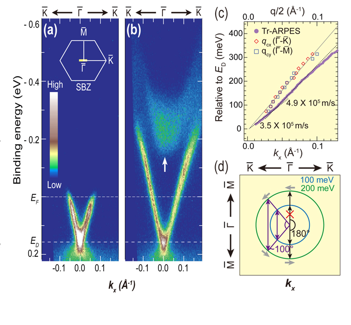
(left) STM image (a), dI/dV image (b), FFT images (c,d) of a cleaved surface of BiSbTeSe. (right) (a,b) band dispersion of TSS studied by pump-and-probe ARPES. (c,d) Large angle scatterings are prohibited.
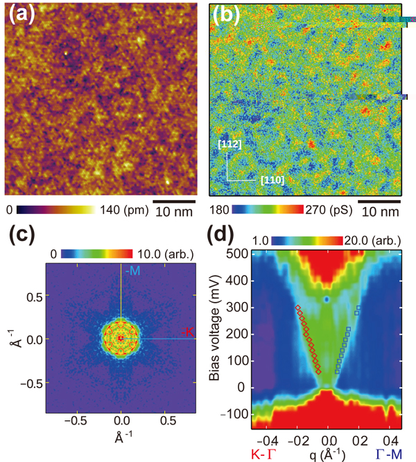
Electronic states of the topological insulator Bi1-xSbx, which is nontrivial in terms of both the Z2 index and the mirror Chern number, were studied by quasiparticle interference (QPI) using low-temperature scanning tunneling spectroscopy. Our Fourier-transform analysis of the QPI patterns reveals the dispersion of the two surface bands above the Fermi energy. Absence of the surface band crossing is unambiguously confirmed, which allowed us to elucidate the mirror Chern number of this system is -1. (details) .
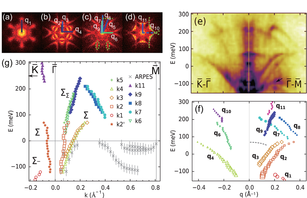
(left) STM image (a), dI/dV curve (b), dI/dV image (c), FFT images (d) of a cleaved surface of Bi1-xSbx. (right) (a-d) Fourie-transformation (FT) of dI/dV
maps at E = -140 (a), -40 (b), +160 (c), and +260(d) meV, (e) FT image in the G-M and
G-K directions. (f) Scattering vectors, (g) Surface band structure.
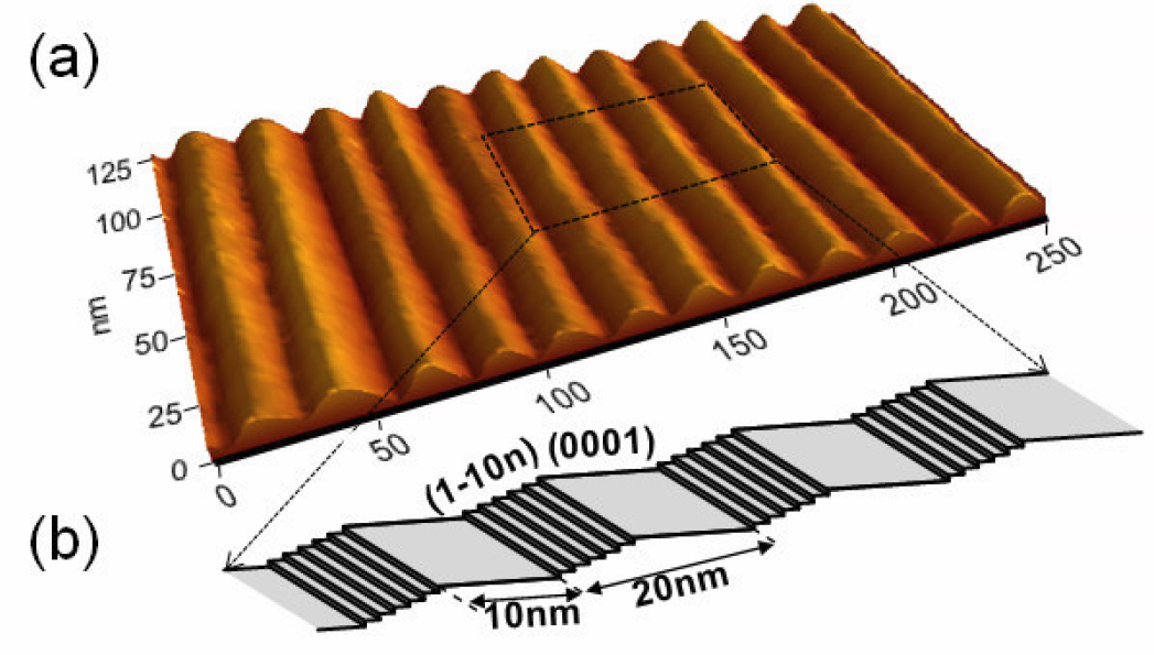
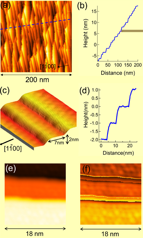
Nanorippled graphene is grown on a macrofacet of SiC(0001) by thermal decomposition. The period of the ripple is confirmed by LEED, STM and replica structure of graphene pi-band ARPES. Inelastic tunneling signals due to graphene phonon excitation modulate according to the period of graphene nanoripple. Presence of graphene nanoribbons at the interface between the surface nanorippled graphene and SiC macrofacet is suggested.
(left) (a) LEED and (b,c) ARPES results at K, (right) (a,b) STM images and (c) inelastic tunneling spectra (d) hight profile, for nanorippled graphene on a macrofacet of SiC(0001).
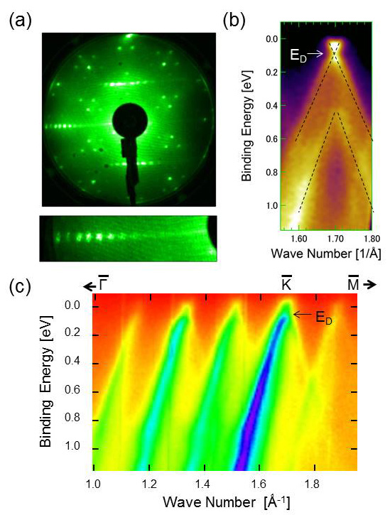
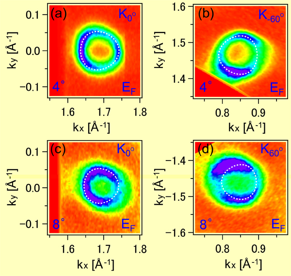
Graphene nanoribbons (GNR) are grown by molecular beam epitaxy on vicinal SiC(0001) substrates, and their electronic structure is studied by ARPES. GNR with armchair edges parallel to the step edge of the substrate covers the terraces of 5-20 nm wide substrate of step-and-terrace structure. The graphene Dirac band shows a band-gap at K-points, the gap size increase with decreasing the ribbon width. (details) .
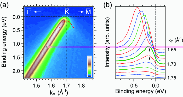
AFM image and the results of ARPES at K for graphene nanoribbon on a 4-degree-off SiC(0001).
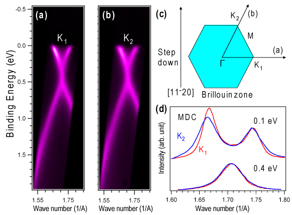
Electronic structure of single-layer graphene grown on a vicinal SiC(0001) is studied. Graphene covers the whole substrate of step-and-terrace structure, and is curved over the step edges. The curved areas induces the scattering of the Dirac electrons as observed in the line width of ARPES (details) . Owing to the electron scattering, the graphene Dirac band on the terrace is elongated in the direction perpendicular to the step edges as observed by ARPES (details) .
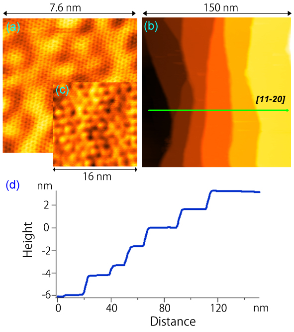
STM images and the results of ARPES for graphene on a 4-degree-off SiC(0001)
STM images of graphene on an 8-degree-off vicinal SiC(0001), and cone shapes of the graphene Dirac band at Fermi energy.
Institute for Solid State Physics , University of Tokyo

Kashiwanoha, Kashiwa-shi, Chiba 277-8581, Japan

Tel +81 4-7136-3310 / FAX +81 4-7136-3474
Last update: 2017/9/1 by komori(AT)issp.u-tokyo.ac.jp